Clearing a Ryobi 18V battery's permanent lockout with a Pi Pico
A Raspberry Pi Pico as a debug probe clears the lockout flag in a Ryobi ONE+ battery's chip, but only after every cell group has measured healthy.
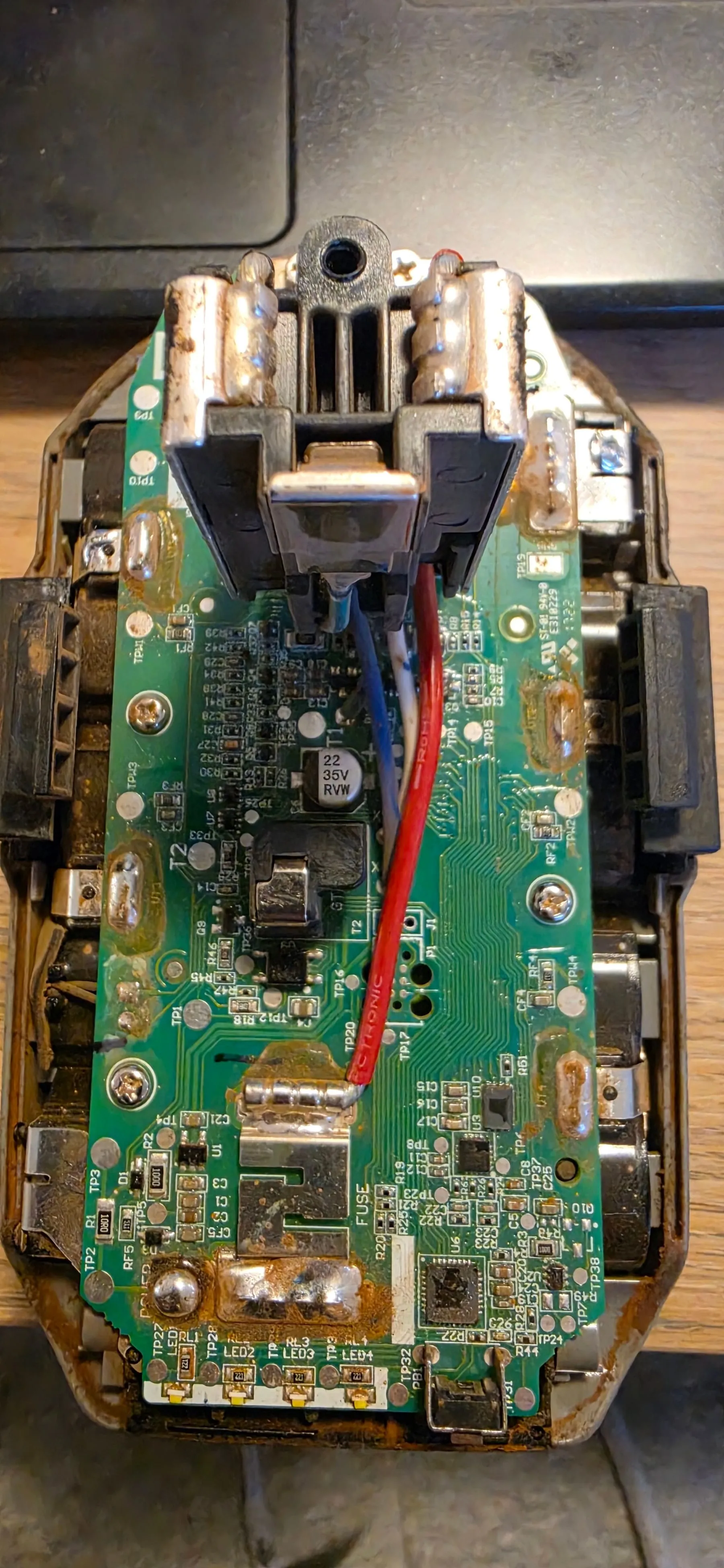
- Difficulty
- Advanced
- Parts cost
- A Raspberry Pi Pico and some jumper wires
- Build time
- An evening, plus charging time
- Skills
- Multimeter, Lithium battery safety, Linux command line, OpenOCD
The problem
This builds on Badar Kayani’s work: his Ryobi battery repair guide and his repair repo, which has the board schematic and locked and fixed copies of the battery firmware. Without those I wouldn’t have known where to start. Two things were different on my pack. The byte that actually changes is at 0x7E94 to 0x7E97: his blog says 0x7E90, which is the start of that row. And my board is a PBP007, where his is a PBP005.
My pack is an 18V ONE+ 6.0Ah HP (model RB1860X). It worked fine with good range. At one bar it went on the charger and sat there for about a week. The next time I picked it up, it was dead and flashed its LEDs 4 times every time I pressed the button.
In Badar’s write-up, about 65% of the dead packs were this firmware lock, not dead cells. The cells can be fine, but the chip on the battery’s board (the BMS, battery management system) has written a “locked” flag into its own memory and won’t let the pack work again. A Ryobi charger won’t clear it. So this is how I cleared that flag, with a Raspberry Pi Pico as the debug probe (the gadget that lets a laptop talk straight to a chip’s memory).
Which lock have you got?
Press the battery’s button and count the flashes:
- 4 flashes every press: an imbalance, a soft lockout or a deep-discharged group. Fix the balance first (see the safety box), then do the J1 reset. Many packs only need that.
- 1 flash, then 4: the permanent lockout. The J1 reset won’t clear it. That’s what the rest of this guide is for.
The J1 reset: press the button, short across J1 on the board, press the button again, LEDs 2 and 4 light up, then remove the short.
Mine showed 4 flashes. I balanced it, did the J1 reset, and it still didn’t come back. When I read the chip, the permanent flag was set. So if J1 doesn’t work, check the flag even if you never saw the single flash.
How it works
The chip is an NXP LPC804, a small ARM microcontroller with 32 KB of flash. The last 1 KB of flash is where the firmware keeps its data, and the lockout flag lives there. The rest is the firmware itself, and I never write to it. The script checks it against my backup before it does anything.
The chip is protected against its serial bootloader (the protection word at 0x2FC reads NO_ISP), so a
USB-serial adapter like a CP2102 can’t do this job. SWD still works. That’s ARM’s two-wire debug
connection, and the Pico speaks it.
The write itself uses the chip’s own built-in flash routines (NXP calls them IAP, in-application programming) rather than OpenOCD’s flash driver. That’s not a style choice: the driver did damage. See the lessons at the bottom.
What you need
- A Raspberry Pi Pico (the original RP2040 one). https://www.raspberrypi.com/products/raspberry-pi-pico/
- The debugprobe firmware,
debugprobe_on_pico.uf2. I used v2.3.1. https://github.com/raspberrypi/debugprobe/releases - A Linux laptop with OpenOCD 0.12:
sudo apt install openocd. OpenOCD is the program that drives the probe. - A multimeter. This is the most important tool here.
- Jumper wires to reach the P1 holes on the board, held so they can’t slip mid-flash. P1 is a Tag-Connect footprint, so a Tag-Connect cable or a pogo-pin clip fits it properly.
- A genuine Ryobi charger for afterwards.
- A non-flammable surface to work on.
- Badar’s repo for the schematic and the reference firmware: https://github.com/bjkayani/ryobi-battery-repair
Wiring
P1 is a Tag-Connect TC2030 footprint: 6 plated holes just below J1. I measured the pinout on my pack. It matches the PBP005 schematic and the standard TC2030 pad layout. Hold the board with the battery button facing you:
            LEFT              RIGHT
 top     6 SWO (unused)    5 GND
 middle  4 SWCLK           3 RESET (3.28 V)
 bottom  2 SWDIO (3.28 V)  1 VCC 3.3 V   ← do NOT connect
TP15 and TP19 are also ground. If you short RESET (middle right) to ground, the chip reboots and the LEDs stay on solid for a while. Don’t, and see the lessons for why it matters.
| Pico pin | Pico GPIO | P1 pin |
|---|---|---|
| 2 | GP1 | 3 RESET |
| 3 | GND | 5 GND |
| 4 | GP2 | 4 SWCLK |
| 5 | GP3 | 2 SWDIO |
The Pico’s 3V3 pin is not connected to anything.
Firmware and config
The probe
Hold the Pico’s BOOTSEL button while you plug it in. It shows up as a USB drive. Copy
debugprobe_on_pico.uf2 onto it, and it restarts as a debug probe.
OpenOCD setup for the LPC804
OpenOCD 0.12 doesn’t recognise the LPC804, so the flash is described by hand. Save this as lpc804.cfg:
# LPC804 (32 KB flash, 1 KB sectors, 4 KB RAM) - OpenOCD 0.12 can't auto-detect its part ID,
# so the flash bank is declared by hand. IAP ROM entry for LPC80x = 0x0F001FF1.
source [find interface/cmsis-dap.cfg]
transport select swd
adapter speed 500
source [find target/swj-dp.tcl]
swj_newdap lpc804 cpu -irlen 4 -expected-id 0
dap create lpc804.dap -chain-position lpc804.cpu
target create lpc804.cpu cortex_m -dap lpc804.dap
lpc804.cpu configure -work-area-phys 0x10000000 -work-area-size 0x800 -work-area-backup 0
flash bank lpc804.flash lpc2000 0x0 0x8000 0 0 lpc804.cpu lpc800 12000 calc_checksum 0x0F001FF1
cortex_m reset_config sysresetreq
gdb_port disabled
telnet_port disabled
tcl_port disabled
backup.sh: read-only
This reads the whole chip twice, checks both copies match, and shows the lockout bytes. It never halts, resets or writes the chip. Run it first, before anything else touches P1.
#!/bin/bash
# READ-ONLY. Dumps the Ryobi BMS LPC804 flash (32 KB) twice via the Pico
# CMSIS-DAP probe, checks both reads match, and shows the lockout bytes.
# Never halts, resets or writes the chip.
set -u
OUT=./dumps
mkdir -p "$OUT"
TS=$(date +%Y%m%d-%H%M%S)
OCD=(openocd -f interface/cmsis-dap.cfg -c "transport select swd; adapter speed 500"
     -c "set CPUTAPID 0" -f target/lpc8xx.cfg)   # LPC804 is M0+ (0x0bc11477), cfg expects M0

echo "== Probe check (reads the chip ID only) =="
timeout 15 "${OCD[@]}" -c "init; shutdown" 2>&1 | grep -E "Info : SWD DPIDR|Error|cortex_m|Cortex-M" || true

for n in 1 2; do
  f="$OUT/ryobi-$TS-read$n.bin"
  echo "== Read $n -> $f =="
  timeout 60 "${OCD[@]}" -c "init; dump_image $f 0x0 0x8000; shutdown" 2>&1 | grep -E "dumped|Error" || true
done

a="$OUT/ryobi-$TS-read1.bin"; b="$OUT/ryobi-$TS-read2.bin"
if [ ! -s "$a" ] || [ ! -s "$b" ]; then echo "FAIL: a read is missing or empty"; exit 1; fi
ls -l "$a" "$b"
if cmp -s "$a" "$b"; then echo "OK: both reads identical ($(sha256sum < "$a" | cut -c1-16))"
else echo "FAIL: reads differ - wiring/contact problem, do NOT write"; exit 1; fi

echo "== CRP word @0x2FC (0xFFFFFFFF/other = no protection) =="
xxd -s 0x2FC -l 4 -e "$a"
echo "== Lockout area @0x7E80-0x7EAF (flag = 0x7E94..0x7E97; blog says 0x7E90) =="
xxd -s 0x7E80 -l 0x30 "$a"
printf "0x7E90..0x7E97 = %s  (locked if 0x7E94-97 not all 00)\n" "$(xxd -s 0x7E90 -l 8 -p "$a")"
What the lockout bytes looked like on my pack and on Badar’s reference images:
| Board | Locked bytes at 0x7E94 | Fixed |
|---|---|---|
| PBP002 (Badar’s) | 24 20 21 20 |
00 00 00 00 |
| PBP004 (Badar’s) | 04 |
00 |
| PBP005 (Badar’s) | 40 |
00 |
| PBP007 (mine) | 20 00 00 00 |
00 00 00 00 |
Your board ID is written in the flash as text at 0x7E40 (PBP007 on mine), so it shows up in the hex
dump.
iap_fix.tcl: the write
This is the part that does the work. It runs inside one OpenOCD session and calls the chip’s own flash routines directly. It only ever erases pages 504 to 507 (0x7E00 to 0x7EFF). The boot block at 0x7F80 to 0x7FFF is never touched.
0x2D4 is my pack’s firmware entry point. Yours may be different. Step 7 below shows how to find it. If it’s different, change all four places it appears.
# Direct LPC804 IAP calls (UM11065 ch.4). Rewrites pages 504-507 (0x7E00-0x7EFF) only.
# Pages 510/511 (0x7F80-0x7FFF) hold the boot block and are never touched.
# Expects: DATA = 256-byte file holding the wanted 0x7E00-0x7EFF contents, EXPECT = full 32 KB expected image.
set CMD  0x10000000
set RES  0x10000020
set BKPT 0x10000040
set BUF  0x10000C00   ;# outside the 0x800 OpenOCD work area, below the IAP stack (0x10000F00)
set IAP  0x0F001FF0

proc rd32 {addr} { return [lindex [read_memory $addr 32 1] 0] }

proc iap {code p0 p1 p2 p3} {
    global CMD RES BKPT IAP
    write_memory $CMD 32 [list $code $p0 $p1 $p2 $p3]
    write_memory $RES 32 {0xFFFFFFFF 0 0 0 0}
    write_memory $BKPT 16 {0xBE00 0xBE00}
    reg r0 $CMD
    reg r1 $RES
    reg sp 0x10000F00
    reg lr [expr {$BKPT | 1}]
    reg pc $IAP
    reg xPSR 0x01000000
    reg primask 1
    resume
    wait_halt 5000
    set st [rd32 $RES]
    echo "  IAP $code ($p0,$p1,$p2) -> status $st"
    if {$st != 0} { error "IAP command $code failed with status $st - stopping" }
}

init
reset halt
echo "== let the boot ROM finish (it trims the 12 MHz FRO the flash timing uses), stop at firmware entry 0x2D4 =="
bp 0x2D4 2 hw
resume
wait_halt 3000
rbp 0x2D4
set pc [lindex [split [reg pc] " "] end]
echo "  stopped at pc=$pc remap=[read_memory 0x40048000 32 1]"
if {$pc != 0x000002d4 && $pc != 0x2d4} { error "did not stop at firmware entry - stopping" }
echo "== pre-check: sectors 1-30 + boot block must match the backup =="
verify_image dumps/code-400-7BFF.bin 0x400 bin
verify_image dumps/bootblock-7F80-7FFF.bin 0x7F80 bin
echo PRECHECK_OK
echo "== load wanted data into RAM =="
load_image $DATA $BUF bin
verify_image $DATA $BUF bin
echo "== prepare sector 31, erase pages 504-507 =="
iap 50 31 31 0 0
iap 59 504 507 0 0
echo "== check pages 504-507 are blank (read as 0) =="
set z [read_memory 0x7E00 32 64]
foreach w $z { if {$w != 0} { error "page not blank after erase" } }
echo "  blank OK"
echo "== prepare + copy 256 bytes RAM -> 0x7E00 =="
iap 50 31 31 0 0
iap 51 0x7E00 $BUF 256 0
echo "== IAP compare flash 0x7E00 vs RAM =="
iap 56 0x7E00 $BUF 256 0
echo "== verify the whole 32 KB against the expected image =="
verify_image $EXPECT 0x0 bin
echo ALL_VERIFIED
reset run
shutdown
In plain words: the IAP command numbers are 50 (prepare the sector for writing), 59 (erase pages), 51 (copy RAM to flash) and 56 (compare flash with RAM). Any status other than 0 stops the script. The pre-check means nothing is written unless the firmware on the chip is exactly the one in my backup.
fix.sh: the wrapper
The chip goes to sleep when nobody’s pressing the battery button, and a sleeping chip doesn’t answer the probe. So this keeps retrying for 90 seconds while you press the button, then runs the whole fix in one go.
#!/bin/bash
# Retries until the chip is awake (battery button), then runs iap_fix.tcl in one session.
cd "$(dirname "$0")"
end=$((SECONDS+90))
echo ">>> PRESS THE BATTERY BUTTON (retrying for 90 s) <<<"
while [ $SECONDS -lt $end ]; do
  LOG=$(timeout 60 openocd -f ./lpc804.cfg -c "set DATA dumps/fix-7E00-7EFF.bin; set EXPECT dumps/expected.bin" -f ./iap_fix.tcl 2>&1)
  grep -q PRECHECK_OK <<<"$LOG" && break
  grep -q "verify_image\|contents differ\|checksum mismatch" <<<"$LOG" && { echo "PRECHECK FAILED - nothing written"; echo "$LOG" | tail -15; exit 1; }
  sleep 0.5
done
echo "$LOG" | grep -v -E "^(Licensed|For bug|	http|Info : CMSIS)"
grep -q ALL_VERIFIED <<<"$LOG" && echo "=== SUCCESS ===" || { echo "=== NOT VERIFIED ==="; exit 1; }
Step by step
- Count the flashes (see “Which lock have you got?” above).
- Open the pack and look at the board.
- Measure every cell group with a multimeter, across each group’s two connection tabs, and write the numbers down. If any group is below 2.5 V, stop here (see the safety box). Mine had one group at 3.25 V and the other four at 3.65 V, so well clear of that. I balanced the low group by hand.
- Check the five small sense resistors the BMS reads each group through (RF1 to RF5 on my board). Mine were fine.
- Try the J1 reset. If the pack comes back, you’re done. Mine didn’t.
- Flash the Pico and wire it up as in the table. Leave 3V3 off. Before you probe P1 with anything
else, run
./backup.shand press the battery button while it runs. It has to end withOK: both reads identical. If the reads differ, it’s a contact problem: fix it and don’t go further. Keep these files somewhere safe. They’re the only way back. - Find your firmware entry point. The backup doesn’t always show the real first bytes of flash: if
the chip is sitting in its boot ROM, the first 512 bytes of the read are the ROM’s start-up table, not
your firmware. Take a “true” read with the chip told to show flash there (SYSMEMREMAP, at 0x40048000,
set to 2). Press the button just before you run it:
Check the output looks like real firmware before you rely on it. The second line prints the firmware’s reset address. Mine wasopenocd -f ./lpc804.cfg -c "init; reset halt; mww 0x40048000 2; dump_image dumps/true-before.bin 0x0 0x8000; reset run; shutdown" xxd -s 4 -l 4 -e dumps/true-before.bin000002d5. Knock the last bit off (ARM chips mark these addresses with an extra 1) and that’s the entry point: 0x2D4. If yours is different, change it iniap_fix.tcl. - Build the fix files from the backup. Use the
read1file from step 6:
The last line must only list addresses from 0x7E94 to 0x7E97. Mine listed one byte:B=dumps/ryobi-YYYYMMDD-HHMMSS-read1.bin # your backup dd if=$B of=dumps/code-400-7BFF.bin bs=1 skip=$((0x400)) count=$((0x7800)) status=none dd if=$B of=dumps/bootblock-7F80-7FFF.bin bs=1 skip=$((0x7F80)) count=128 status=none dd if=$B of=dumps/fix-7E00-7EFF.bin bs=1 skip=$((0x7E00)) count=256 status=none printf '\x00\x00\x00\x00' | dd of=dumps/fix-7E00-7EFF.bin bs=1 seek=$((0x94)) conv=notrunc status=none cp $B dumps/expected.bin printf '\x00\x00\x00\x00' | dd of=dumps/expected.bin bs=1 seek=$((0x7E94)) conv=notrunc status=none cmp -l $B dumps/expected.bin | awk '{printf "0x%04X %s -> %s (octal)\n", $1-1, $2, $3}'0x7E94 40 -> 0 (octal), which is 0x20 to 0x00. The expected image is built from thebackup.shread, not the true read, because that’s how the chip looks to the final check in the script. That’s what worked on mine. - Run
./fix.shand press the battery button while it retries. It must end in=== SUCCESS ===. If it saysPRECHECK FAILED - nothing written, the chip doesn’t match your backup. Stop and work out why before you try again. - Take another true read and compare (see Testing it).
- Take the probe off, do a J1 reset, and charge it on a Ryobi charger, on that non-flammable surface, with you there.
- Write it down. Model, board ID, firmware entry, the lockout bytes, group voltages on arrival, what you did and what happened. I’m keeping one row per pack. Every pack I log tells me something the last one didn’t.
Testing it
The test that counts is a fresh read of the chip compared with the one from before. Press the button, then:
openocd -f ./lpc804.cfg -c "init; reset halt; mww 0x40048000 2; dump_image dumps/true-after.bin 0x0 0x8000; reset run; shutdown"
cmp -l dumps/true-before.bin dumps/true-after.bin | awk '{printf "0x%04X %s -> %s (octal)\n", $1-1, $2, $3}'
Only 0x7E94 to 0x7E97 may show up. On mine, the only difference in the whole 32 KB was 0x7E94. I read it twice and both reads matched.
Where mine is up to, honestly: the flag is cleared and the chip checks out. What I haven’t finished yet is proving the pack itself is healthy. The checks I’m running:
- Self-discharge: charge it full, measure all five groups, leave it off the charger, and measure again at 3 days and 7 days. If they all hold, the lock was probably a glitch. If one group falls behind, that group is bad.
- Sag under load: measure each group while a tool is working hard. A group that drops well below the others has high internal resistance (it can’t deliver current like the rest).
- Re-read the chip’s log after use. The firmware seems to keep a minimum and maximum for each group at 0x7E50. If those numbers move in line with what the meter saw, that’s what the block really is.
Lessons learnt
OpenOCD’s flash writer erased more than I asked for. OpenOCD 0.12’s flash driver doesn’t know the
LPC804 (it reports the part as “unknown”), so it writes the whole 1 KB last sector, including the two
pages at the end that hold the chip’s boot block. Those can’t be erased, so the chip refuses with an
error. But by then the driver has already erased. Don’t use flash write_image on this chip. Call the
chip’s own IAP routines and erase only the pages you mean to, like iap_fix.tcl does.
An erase straight after a reset only half worked, and said it had worked. After reset halt, the
chip stops on the very first instruction of its boot ROM, before the ROM has trimmed the internal clock
(the FRO, the chip’s built-in oscillator) that the flash erase is timed from. The erase pulse runs too
short and the bits only half clear. The IAP call still returns 0, success, and the data is scrambled.
The fix is to let the boot ROM finish: put a breakpoint on the firmware’s reset handler (0x2D4 on mine),
let it run, and do the flash work from there.
Blank flash on this chip reads 0x00, not 0xFF. Most flash reads 0xFF when it’s erased. Check for the right one, or your “is it blank?” test passes when it shouldn’t, or fails when it shouldn’t.
OpenOCD’s stock LPC8xx setup expects the wrong chip ID. The LPC804 has a Cortex-M0+ core, and the
stock config expects a plain M0’s ID. set CPUTAPID 0 (or -expected-id 0 in my own config) tells it
not to check.
The chip goes to sleep and takes the probe with it. When idle, the chip sleeps and the debug
connection stalls (“stalled AP operation”). Holding it in reset doesn’t help either: then it doesn’t
answer at all. Press the battery button, halt it, and do everything in one session. That’s why
fix.sh retries until you press the button.
Keep your RAM buffers out of OpenOCD’s working area. verify_image runs a small checking routine
in the chip’s RAM. If your data is sitting in the same spot, the check overwrites it. My buffer is at
0x10000C00, above OpenOCD’s 0x800-byte area.
The address in the blog is the start of the row. Badar’s blog gives 0x7E90. When I compared his locked and fixed images byte by byte, the bytes that actually change start at 0x7E94. Zero 0x7E94 to 0x7E97 and leave the rest of the row alone.
I muddied my own evidence. Before I’d taken a backup, I put my meter’s continuity test across RESET and ground on P1 by accident. The LEDs went solid and stayed on. When I connected the probe after that, the chip was crashed in its boot ROM. That crash most likely came from my slip, not the lock, so it tells me nothing about why the pack locked. (The pack was already locked before I opened it, so the flag itself wasn’t my doing.) Take the backup and read the lockout and log bytes before any reset or probing on P1. Then the state the pack arrived in is real evidence.
A lock usually has a reason, but don’t guess it from one reading. The block at 0x7E50 on my pack looks like a min/max log per group, and one group’s minimum was 1613 mV. That’s probably what set the lock, so I treat that group as suspect. But the other groups’ “minimums” were around 2.4 V, which can’t be resting voltages on a pack that was working well. So it’s more likely sag under load, which points to a group with high internal resistance rather than one that was run flat. I haven’t proven which yet.
One pack isn’t a pattern. I was tempted to write a tool that does all of this in one click. I haven’t, and I’m not patching the hard lock out of the firmware either. A tool built from one pack would fail on exactly the odd cases this one threw at me, and the hard lock is what protects cells that really have been run flat. I’m logging every pack first: model, board ID, firmware entry, lockout bytes, group voltages and outcome. Once there’s enough variation in that log, a tool might make sense.